This is an old revision of the document!
Table of Contents
/* Imported from Wayback Machine
 Original URL : https://retrobrewcomputers.org/doku.php?id=boards:ecb:zilog-peripherals:start
 Snapshot date: 2021-01-17
 Generator    : wayback-archiver
*/
ECB Zilog Peripherals
Introduction
The Zilog Peripherals board adds Zilog Z80 family serial and counter timer peripherals I/O chips to an existing ECB Z80 SBC or N8 computer.
Pictures

Specifications
Two serial ports using Z80-DART or Z80-SIO
Baud rates can be jumper selected or use Z80-CTC channels for software programmable
Four parallel ports with handshaking using two Z80-PIO
Four counter / timers using Z80-CTC
Daisy chained priority interrupts for Z80 mode 2 operation
Acknowledgments
The ECB ZILOG Peripherals board is based on a design presented in c't magazine in 1985 “Datenverkehr - Die I/O-Karte fur den ECB-Bus” by Georg Umback. The original documentation for this project can be seen here: :boards:ecb:zilog-peripherals:zp_dart_sio_ct8504.pdf
Andrew Lynch designed the current version with David Giles and Douglas Goodall assisting with testing on the SBC V1 & V2 respectively.
Version
The following documentation and files describe version 2 which has not been manufactured and tested as at 29/11/2019. Version 2 adds a jumper to bridge CTC counter 2 and 3 so that CTC counter 2 can be used as a prescaler. The serial headers connectors have been reconfigured to the IBM PC standard. A reset configuration jumper has been added to allow selection of either KONTRON or Legacy (N8VEM) reset method.
Details on prior versions can be can be found here.
Hardware Documentation
Schematics
Board Layout
KiCad Files
PCB Gerber files

Connectors
X1 - PIO1
X2 - PIO2
X3 - DART/SIO channel B (RS-232 levels)
X4 - CTC, DART/SIO channel A (TTL levels)
X5 - oscillator divider selection
X6 - DART/SIO baud rate clock source selection
X7 - DART/SIO channel A (RS-232 levels)
Hardware Documentation
Board address
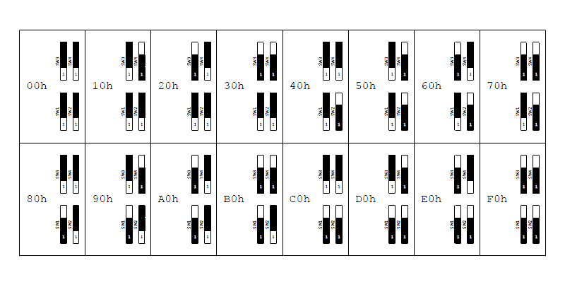
The board occupies 16 I/O addresses. The base address is selected by the jumpers labeled SW1 to SW4 near the ECB connector. All jumpers need shorting headers to select the desired address range. If used with an N8 computer it is generally safe to use address ranges A0h and above. Not all possible conflicts are shown as many of the ECB boards have flexible address selection. The photo shows the board set for 10h to 1Fh.
Base Address | SW1 (A7) | SW2 (A6) | SW3 (A5) | SW4 (A4) | Conflicts |
00h | 2-3 | 2-3 | 2-3 | 2-3 | I/O on N8 CPU after reset |
10h | 2-3 | 2-3 | 2-3 | 1-2 | |
20h | 2-3 | 2-3 | 1-2 | 2-3 | Used for Disk I/O IDE |
30h | 2-3 | 2-3 | 1-2 | 1-2 | Used for Disk I/O Floppy |
40h | 2-3 | 1-2 | 2-3 | 2-3 | N8 CPU registers |
50h | 2-3 | 1-2 | 2-3 | 1-2 | N8 CPU registers |
60h | 2-3 | 1-2 | 1-2 | 2-3 | Used by Z80 SBC I/O |
70h | 2-3 | 1-2 | 1-2 | 1-2 | Used by Z80 SBC I/O |
80h | 1-2 | 2-3 | 2-3 | 2-3 | N8 I/O default |
90h | 1-2 | 2-3 | 2-3 | 1-2 | N8 I/O default |
A0h | 1-2 | 2-3 | 1-2 | 2-3 | |
B0h | 1-2 | 2-3 | 1-2 | 1-2 | |
C0h | 1-2 | 1-2 | 2-3 | 2-3 | |
D0h | 1-2 | 1-2 | 2-3 | 1-2 | |
E0h | 1-2 | 1-2 | 1-2 | 2-3 | |
F0h | 1-2 | 1-2 | 1-2 | 1-2 | ECB VDU I/O |
Visual guide for I/O address setting:
Z80-PIO
The Z80-PIOs provide two 8-bit parallel ports each. Each Z80-PIO has its own header with 5v and GND lines for connecting to the outside world. Note these connectors have a totally different layout to the PPI connectors on other boards. No jumpers need to be set to use these Z80-PIOs.
Interrupts
The /INT pins from the Z80-DART/SIO, Z80-CTC and Z80-PIOs are connected together as a 'wired-OR' gate and buffered for a common interrupt to the CPU. These pins are open-drain outputs so they can be connected together. The board is setup for Mode 1 or Mode 2 interrupts. The four chips are also daisy chained to give priority to the interrupts. The Z80-CTC has the highest priority, followed by the Z80-DART/SIO, Z80-PIO1 and lowest is Z80-PIO2. Z80-CTC channel 3 is ideal for use as a 'general' mode 2 interrupt as it doesn't have an output pin.
For example, to use the UART on the Z80-SBC MK-II board with mode 2 interrupts requires a jumper setting and a hardware modification. On the N8VEM Z80-SBC MK-II jumper pins 2-3 on k12. This connects the UART interrupt to A23 on the ECB connector. On the Zilog peripherals board solder a bridge between A23 on the ECB connector and pin 20 of the Z80-CTC. Alternatively solder to pin 11 of header X4 and jumper pins 9-11 to connect to the Z80-CTC. The N8VEM Z80-SBC MK-I requires more modifications and is not covered here.
Initial Testing
For this section I will assume the base address of the board is B0h, the oscillator module at U8 is 4.9152MHz. On X5 there are jumpers between 7-8 and 15-16 to give a baud rate of 9600. On X6 jumper pins 3-5 and 8-10 to put the baud rate clock to the Z80-DART/SIO. If available use a frequency counter to measure 153600Hz at pins 13, 14 and 27 of the Z80-DART/SIO.
Testing the Z80-CTC
On X6 put a jumper on pins 2-4 to put the 153600Hz signal to channel 0. Using DBGMON send the following to the Z80-CTC. (Text in blue is what you type)
>O B0 47
>O B0 00
>O B1 27
>O B1 00
The first command sets channel 0 as a counter, the second sets the count value to 256. The output on pin 7 of the Z80-CTC should be 600Hz (153600 / 256). The third and fourth commands set channel 1 as a timer which divides the system clock by 65536. Given my setup has the CPU running at 4MHz the output on pin 8 of the Z80-CTC should be a bit over 61Hz (4000000/65536). The outputs are not a square wave but a series of pulses and were too short to be picked up by my ancient logic probe. However they measured correctly on my frequency counter. An oscilloscope would be handy as well.
Testing the Z80-DART/SIO
I am using a SIO/0 on my board. The DART uses the same register layout except the synchronous stuff is missing.
Loopback test. Install a jumper between pins 3 and 5 of X7 to connect TxD with RxD of channel A. Using DBGMON send the following:
>O B6 04 select write register 4
>O B6 46 x16 clock, 1 stop, no parity
>O B6 01 select write register 1
>O B6 04 disable interrupts
>O B6 03 select write register 3
>O B6 C1 8 bits, no auto enables, receiver enable
>O B6 05 select write register 5
>O B6 EA DTR on, RTS on, enable transmit
Next check the status by
>I B6
Bit 6 is set after a chip reset and is cleared with
>O B6 C0
If bit 2 (Tx pending) is set then we're ready to transmit, so
>O B4 40
will send the character 40 (@) to the transmit buffer. Then read status and bit 0 should be set to indicate a character has been received. Read it with
>I B4
and the result should be 40. If not then try again as it could be leftover crud in the receive buffer.
Once the loopback test is successful then take out the jumper in X7, put in your carefully constructed serial lead and try it with a terminal.
Testing the Z80-PIOs
After reset the Z80-PIOs will have their ports set to mode 1 (all inputs). Using the monitor to read the four ports at 0xB8, 0xB9, 0xBC and 0xBD (i.e.I B8) will read the values on the pins. With nothing connected to headers X1 and X2 my Z80-PIOs read all zeros. A clip lead from the 5 to any I/O pin will show up as a different value when the port is read.
A simple register test program is available (base address 0xB0): :boards:ecb:zilog-peripherals:2piotst.zip
At this stage you should have a functioning Zilog Peripheral Board. Combined with the SBC V2 you now have enough serial ports, timers and parallel ports to create a working MP/M system. Any takers?
Using the Z80-PIO with a Centronics printer.
The Z80-PIO has four modes of operation - input, output, bi-directional and bit. The input and output modes have handshaking pins for each port, the bi-directional mode (port A only) uses handshaking pins from both ports and bit mode uses no handshaking pins. For a printer the output mode is used with the port's RDY pin used as a strobe output and the /STB pin used as an ACK input. However the RDY signal is too short (and the wrong polarity) for the printer. This signal is used to trigger a monostable (say a 74LS123) with an active low output pulse about 0.5mS long. The BUSY signal and other control lines go to/from the other port in bit mode.
Buffering the data and control lines are needed for long cables. Use a 74LS245 or similar for the data lines, a 74LS07 or similar for the control lines.
The above idea has been prototyped and may become a future mini-board.
Resources
Filename
Filesize Last modified 2piotst.zip 3.4 KiB 2018/09/24 10:21 ctctimer.gif 99.4 KiB 2020/01/29 05:57 ecb_zilog_peripherals-004.zip 29.8 KiB 2018/04/22 11:50 ecb_zilog_peripherals.zip 173.0 KiB 2019/11/18 07:00 ecb_zilog_peripherals_gerbers.zip 87.9 KiB 2019/11/18 07:06 img_8617.jpg 784.6 KiB 2018/04/22 11:14 img_8618.jpg 773.7 KiB 2018/04/22 11:30 img_8622.jpg 747.9 KiB 2018/04/22 11:31 img_8626.jpg 1.4 MiB 2018/04/22 11:34 img_8627.jpg 1.3 MiB 2018/04/22 11:35 img_8640.jpg 730.9 KiB 2018/04/22 11:36 img_8644.jpg 1.4 MiB 2018/04/22 11:37 img_8645.jpg 1.4 MiB 2018/04/22 11:39 img_8646.jpg 1.3 MiB 2018/04/22 11:40 img_8647.jpg 1.5 MiB 2018/04/22 11:41 n8vem-zilogperiph-back-300dpi.png 3.7 MiB 2018/04/22 11:45 n8vem-zilogperiph-front-300dpi.png 3.9 MiB 2018/04/22 11:49 z80-interrupts.pdf 897.7 KiB 2018/04/22 13:06 z80_kio.pdf 345.6 KiB 2018/04/22 13:05 z80_peripherals.pdf 2.3 MiB 2018/04/22 13:06 z80_pio.pdf 616.3 KiB 2018/04/22 13:06 z84015_ipc.pdf 1.9 MiB 2018/04/22 13:06 zilog-peripherals-jumpers.png 13.2 KiB 2018/07/16 09:56 zilog_peripherals-board-2.0_002.pdf 425.4 KiB 2019/11/29 07:44 zilog_peripherals-board.pdf 239.7 KiB 2018/04/22 12:12 zilog_peripherals-full-board.pdf 439.0 KiB 2018/04/23 00:40 zilog_peripherals-gerbers-2.0_002.zip 281.0 KiB 2019/11/29 07:34 zilog_peripherals-kicad-2.0_002.zip 426.9 KiB 2019/11/29 07:57 zilog_peripherals-schematic.pdf 184.9 KiB 2018/04/22 12:13 zilog_peripherals-schematics-2.0_002.pdf 258.4 KiB 2019/11/29 07:38 zilog_pio_technical_manual.pdf 25.8 MiB 2018/04/22 12:09 zilog_sio_technical_manual.pdf 24.1 MiB 2018/04/22 12:46 zilogperipheral1.jpg 470.2 KiB 2018/04/22 12:17 zp-dw.jpg 1.9 MiB 2019/11/09 02:43 zp_dart_sio_ct8504.pdf 39.5 MiB 2018/04/22 13:02 zp_dart_sio_ct8504_4_english.doc 46.0 KiB 2018/04/22 12:20 zp_dart_sio_ct8504_4_german.rtf 27.1 KiB 2018/04/22 13:07 zp_dart_sio_ct8504_asm.pdf 24.1 KiB 2018/04/22 12:33 zp_in.docx 20.1 KiB 2018/04/22 12:23 zp_z80_dart_uart_pin.pdf 879.0 KiB 2018/04/22 12:52 zp_zilog-peripherals.zip 5.4 KiB 2018/04/22 12:30 zp_zilog_peripherals.txt 1.5 KiB 2018/04/22 12:50 zp_zilog_peripherals_init.txt 1.6 KiB 2018/04/22 12:50 zp_zilog_z80_cpu_peripherals.pdf 1.6 MiB 2018/04/22 13:07